- 您现在的位置:买卖IC网 > Sheet目录443 > IRF540NL (International Rectifier)MOSFET N-CH 100V 33A TO-262
�� �
�
�IRF540NS/IRF540NL�
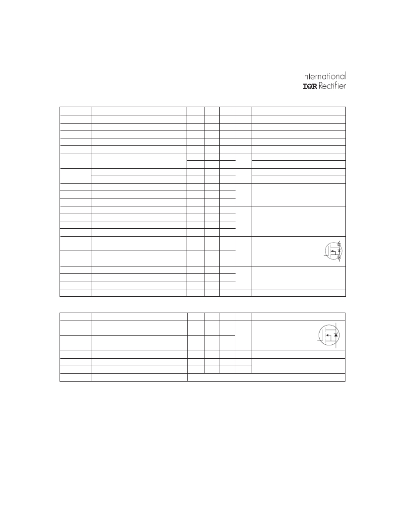
�Electrical� Characteristics� @� T� J� =� 25°C� (unless� otherwise� specified)�
�Parameter�
�Min.� Typ.� Max.� Units�
�Conditions�
�V� (BR)DSS�
�Drain-to-Source� Breakdown� Voltage�
�100� –––� –––� V� V� GS� =� 0V,� I� D� =� 250μA�
�?� V� (BR)DSS� /� ?� T� J�
�Breakdown� Voltage� Temp.� Coefficient�
�–––�
�0.12� –––�
�V/°C�
�Reference� to� 25°C,� I� D� =� 1mA� ?�
�R� DS(on)�
�Static� Drain-to-Source� On-Resistance�
�–––� –––� 44� m� ?�
�V� GS� =� 10V,� I� D� =� 16A�
�?�
�μA�
�–––� –––� 100� V� GS� =� 20V�
�V� GS(th)�
�g� fs�
�I� DSS�
�I� GSS�
�Q� g�
�Q� gs�
�Gate� Threshold� Voltage�
�Forward� Transconductance�
�Drain-to-Source� Leakage� Current�
�Gate-to-Source� Forward� Leakage�
�Gate-to-Source� Reverse� Leakage�
�Total� Gate� Charge�
�Gate-to-Source� Charge�
�2.0� –––� 4.0� V� V� DS� =� V� GS� ,� I� D� =� 250μA�
�21� –––� –––� S� V� DS� =� 50V,� I� D� =� 16A� ?� ?�
�–––� –––� 25� V� DS� =� 100V,� V� GS� =� 0V�
�–––� –––� 250� V� DS� =� 80V,� V� GS� =� 0V,� T� J� =� 150°C�
�nA�
�–––� –––� -100� V� GS� =� -20V�
�–––� –––� 71� I� D� =� 16A�
�–––� –––� 14� nC� V� DS� =� 80V�
�–––� 35� –––� I� D� =� 16A�
�–––� 39� –––� R� G� =� 5.1� ?�
�Q� gd�
�t� d(on)�
�t� r�
�t� d(off)�
�t� f�
�Gate-to-Drain� ("Miller")� Charge�
�Turn-On� Delay� Time�
�Rise� Time�
�Turn-Off� Delay� Time�
�Fall� Time�
�–––� –––� 21� V� GS� =� 10V,� See� Fig.� 6� and� 13�
�–––� 11� –––� V� DD� =� 50V�
�ns�
�–––� 35� –––� V� GS� =� 10V,� See� Fig.� 10� ?� ?�
�??�
�L� D�
�L� S�
�Internal� Drain� Inductance�
�Internal� Source� Inductance�
�–––�
�–––�
�4.5� –––�
�7.5� –––�
�nH�
�Between� lead,�
�6mm� (0.25in.)�
�from� package�
�and� center� of� die� contact�
�G�
�D�
�S�
�C� iss�
�C� oss�
�C� rss�
�E� AS�
�Input� Capacitance�
�Output� Capacitance�
�Reverse� Transfer� Capacitance�
�Single� Pulse� Avalanche� Energy� ??�
�–––� 1960� –––� V� GS� =� 0V�
�–––� 250� –––� V� DS� =� 25V�
�–––� 40� –––� pF� ?� =� 1.0MHz,� See� Fig.� 5� ?�
�–––� 700� ?� 185� ?� mJ� I� AS� =� 16A,� L� =� 1.5mH�
�Source-Drain� Ratings� and� Characteristics�
�Parameter�
�Min.� Typ.� Max.� Units�
�Conditions�
�A�
�integral� reverse�
�p-n� junction� diode.�
�I� S�
�I� SM�
�V� SD�
�Continuous� Source� Current�
�(Body� Diode)�
�Pulsed� Source� Current�
�(Body� Diode)� ?�
�Diode� Forward� Voltage�
�MOSFET� symbol�
�–––� –––� 33�
�showing� the�
�G�
�–––� –––� 110�
�–––� –––� 1.2� V� T� J� =� 25°C,� I� S� =� 16A,� V� GS� =� 0V� ?�
�D�
�S�
�t� rr�
�Q� rr�
�t� on�
�Notes:�
�Reverse� Recovery� Time�
�Reverse� Recovery� Charge�
�Forward� Turn-On� Time�
�–––� 115� 170� ns� T� J� =� 25°C,� I� F� =� 16A�
�–––� 505� 760� nC� di/dt� =� 100A/μs� ??�
�Intrinsic� turn-on� time� is� negligible� (turn-on� is� dominated� by� L� S� +L� D� )�
�?� Repetitive� rating;� pulse� width� limited� by�
�max.� junction� temperature.� (See� fig.� 11)�
�?� Starting� T� J� =� 25°C,� L� =1.5mH�
�R� G� =� 25� ?� ,� I� AS� =� 16A.� (See� Figure� 12)�
�?� I� SD� ≤� 16� A� ,� di/d� t� ≤� 340A/μs,� V� DD� ≤� V� (BR)DSS� ,�
�T� J� ≤� 175°C�
�?� Pulse� width� ≤� 400μs;� duty� cycle� ≤� 2%.�
�2�
�?� This� is� a� typical� value� at� device� destruction� and� represents�
�operation� outside� rated� limits.�
�?� This� is� a� calculated� value� limited� to� T� J� =� 175°C� .�
�?� Uses� IRF540N� data� and� test� conditions.�
�**When� mounted� on� 1"� square� PCB� (FR-4� or� G-10� Material).� For�
�recommended� footprint� and� soldering� techniques� refer� to� application�
�note� #AN-994�
�www.irf.com�
�发布紧急采购,3分钟左右您将得到回复。
相关PDF资料
IRF540STRR
MOSFET N-CH 100V 28A D2PAK
IRF5800TRPBF
MOSFET P-CH 30V 4A 6-TSOP
IRF5804TRPBF
MOSFET P-CH 40V 2.5A 6-TSOP
IRF6100PBF
MOSFET P-CH 20V 5.1A FLIPFET
IRF6100
MOSFET P-CH 20V 5.1A FLIP-FET
IRF6215L
MOSFET P-CH 150V 13A TO-262
IRF634B_FP001
MOSFET N-CH 250V 8.1A TO-220
IRF640NL
MOSFET N-CH 200V 18A TO-262
相关代理商/技术参数
IRF540NLHR
制造商:International Rectifier 功能描述:Trans MOSFET N-CH 100V 33A 3-Pin(3+Tab) TO-262 制造商:International Rectifier 功能描述:TRANS MOSFET N-CH 100V 33A 3PIN TO-262 - Bulk
IRF540NLPBF
功能描述:MOSFET MOSFT 100V 33A 44mOhm 47.3nC RoHS:否 制造商:STMicroelectronics 晶体管极性:N-Channel 汲极/源极击穿电压:650 V 闸/源击穿电压:25 V 漏极连续电流:130 A 电阻汲极/源极 RDS(导通):0.014 Ohms 配置:Single 最大工作温度: 安装风格:Through Hole 封装 / 箱体:Max247 封装:Tube
IRF540NPBF
功能描述:MOSFET MOSFT 100V 33A 44mOhm 47.3nC RoHS:否 制造商:STMicroelectronics 晶体管极性:N-Channel 汲极/源极击穿电压:650 V 闸/源击穿电压:25 V 漏极连续电流:130 A 电阻汲极/源极 RDS(导通):0.014 Ohms 配置:Single 最大工作温度: 安装风格:Through Hole 封装 / 箱体:Max247 封装:Tube
IRF540NS
制造商:International Rectifier 功能描述:MOSFET N D2-PAK
IRF540NS_05
制造商:IRF 制造商全称:International Rectifier 功能描述:HEXFET㈢ Power MOSFET
IRF540NSHR
制造商:International Rectifier 功能描述:Trans MOSFET N-CH 100V 33A 3-Pin(2+Tab) D2PAK 制造商:International Rectifier 功能描述:TRANS MOSFET N-CH 100V 33A 3PIN D2PAK - Rail/Tube
IRF540NSPBF
功能描述:MOSFET 100V 1 N-CH HEXFET 44mOhms 47.3nC RoHS:否 制造商:STMicroelectronics 晶体管极性:N-Channel 汲极/源极击穿电压:650 V 闸/源击穿电压:25 V 漏极连续电流:130 A 电阻汲极/源极 RDS(导通):0.014 Ohms 配置:Single 最大工作温度: 安装风格:Through Hole 封装 / 箱体:Max247 封装:Tube
IRF-540NSPBF
制造商:International Rectifier 功能描述: